Sign up for newsletters
Stay up to date on the weekly newsletters on recent news and activities.
25.07.2023 - Photonics & Smart materials, Technology
Semiconductors or chips are essential components in modern technology, powering everything from smartphones and computers to cars and medical devices. Manufacturing them is a highly specialized multi-step process, which begins with melting/purifying silicon into crystal ingots. These ingots are then sliced into thin wafers – the material upon which the chip circuitry is formed.
Dr. Anatoly Kravstov – a scientist, engineer, and the Managing Director of Kepp EU – has been producing silicon ingots for several decades. In 2011, he established his company in Latvia to tap into the European market and has since been developing a new ingot production method that is uniquely suited to meet surging demand for larger diameter wafers.
Labs of Latvia visited the Kepp EU factory, where Anatoly told us about his new method and future ambitions.
In layman’s terms, silicon ingots are produced by melting silicon and then allowing it to solidify into a uniform cylindrical shape. Depending on the method used, the silicon ingot can vary in purity and size.
Purity matters because, generally speaking, the fewer contaminations in the wafer, the better it performs. Going into the future, high-performance chips and sensors will increasingly demand higher purity silicon.
Anatoly points out that the microelectronics market is set to grow 3-5-fold through 2030 and will require larger diameter silicon ingots to satisfy growing consumption. Size matters because wider wafers dramatically improve production efficiency, reduce cost, and enable more complex and powerful microchips.
With the current production methods – Czochralski (CZ) and Float Zone (FZ) – there is a tradeoff between size, purity, and cost, namely, the CZ method can create large diameter crystals more cost-efficiently, but they’re less pure than those created by the FZ method.
There is also a modified version of CZ, known as the Magnetic Czochralski method (MCZ), that leverages a magnetic field to decrease interaction between the silicon melt and the crucible walls. However, the energy required to sustain the magnetic field throughout the process massively increases the costs to the point where it has very limited application and is only used for specific products.
In short, the semiconductor industry needs purer and larger diameter wafers – a need that current production methods cannot meet cost-efficiently.
“If at all, as MCZ & FZ silicon growth technologies encounter fundamental physical limitations when scaling ingots up to a diameter of 300mm,” says Anatoly.
That’s where Kepp EU comes in.
Over more than a decade of work, Anatoly has developed a novel approach to silicon ingot production that he has dubbed the Electron Beam Zone method (EBZ), which, as the name suggests, is designed to use electron beam heating for the melting process.
“We have developed the EBZ process, which is revolutionizing silicon crystal growth. You can think of it in terms of the evolution of engines: CZ is a car with a gasoline engine, the FZ process is a diesel car, whereas the EBZ process is the evolutionary leap – the electric car,” Anatoly explains.
EBZ enables the production of larger diameter wafers (300mm) at high purity (oxygen contents of <0,1 ppma – or more on customer request) and no graphite much more cost-effectively (nearly 2x cheaper than FZ per product kg).
Anatoly has already successfully created growing rods using the EBZ process. This new method is protected by 12 patents and has been described in 30 scientific articles.
However, there’s still a way to go before growing the type of silicon single crystals that are suitable for high-purity wafer production.
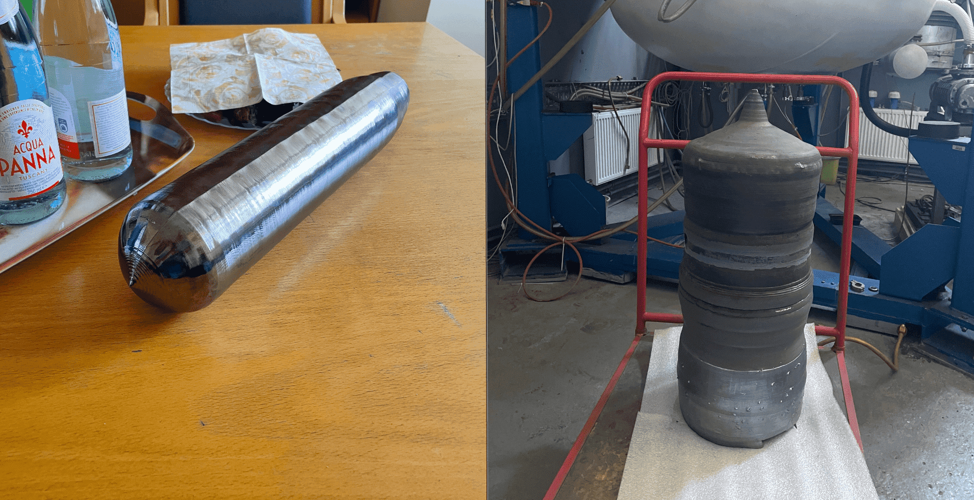
On the left: a silicon ingot produced through the FZ method. On the right: a silicon ingot produced through the EBZ method. Both made by KEPP EU.
“We can create 300mm crystals. We have the equipment for pulling ingots and the design for modernizing the machine. Now, we’re looking for investments,” says Anatoly.
To begin production, the gas-vacuum system of the puller must be modernized and crystal growth control programs optimized. It’s no small task and comes with a hefty price tag. For instance, suitable industrial-grade vacuum pumps come at a premium price and Anatoly estimates a €2.1M investment is required to complete the machine and the technology for growing 300mm ingots of the required quality.
“To turn the factory into an export-ready producer of high-quality ingots, we’re looking at no less than €14M in investments needed. That is to start production of 300mm ingots with a low level of contamination – the type required by Europe – in the next five years.”
It’s no secret that Europe is scrambling to boost its semiconductor production. Pandemic supply chain issues and current geopolitical turbulence have illuminated the importance of this technology’s strategic and economic value.
Currently, Europe manufactures about 10% of the global supply of semiconductors and has committed €43B as part of its Chips Act to develop and bolster the European chip industry with the goal of doubling its global share.
In a bid to throw its name in the hat for Latvia’s participation in Europe’s chip sovereignty push, a Memorandum of Understanding (MoU) was signed at the end of 2022 by 10 partners – universities, institutes, leading Latvian tech companies, and relevant public institutions.
The memorandum is made up of three key components:
So, is Latvia on course to become a full-fledged chip manufacturer?
“No,” says Anatoly. “To go from raw material to a finished chip, there are dozens of steps, each more expensive than the last. Investments needed for each phase are measurable in hundreds of millions, even billions of dollars. To develop an end-to-end semiconductor manufacturing process in Latvia, you would need massive funds. This is to say nothing of the deep and diverse expertise required to make it all a reality.”
To put it into perspective, Infineon – Germany’s largest semiconductor manufacturer – is building a new factory in Dresden for semiconductor wafers (wafers and chips) at a project cost of €5B. And this is with decades of experience and expertise as one of the world’s top 10 largest manufacturers.
“For Latvia, it may be more realistic to focus on a particular link or two in the value chain, for example, the production of silicon ingots and the dicing of finished semiconductor wafers into chips, and packaging. Or master the development of chip design, followed by an OEM for the production of silicon, and then semiconductor wafers,” says Anatoly.
So, does Latvia have a role to play in Europe’s push for chip independence? Anatoly suggests we should double down on the foundations we already have.
“Latvia could supply all of Europe with 300mm wafers. Work with me, let’s put up one factory and for some €100-150M we can make Latvia the silicon wafer capital of Europe. This would be possible, for example, in the Liepāja Special Economic Zone,” laughs Anatoly, with a hopeful smile that signals he dreams of realizing such production in Latvia.
Source: Press release (www.labsoflatvia.com)
Photo: Dr. Anatoly Kravstov in front of his invention
Stay up to date on the weekly newsletters on recent news and activities.
Stay up to date on the weekly newsletters on recent news and activities.